Ga naar Gerards page / go to Gerards other pages ---->>> ![]()

Refurbishing a Sansui AU555, january 2025
![]() Gemakshalve is deze pagina alleen in het Engels geschreven.
Gemakshalve is deze pagina alleen in het Engels geschreven.
![]() This page was written using English language only.
This page was written using English language only.
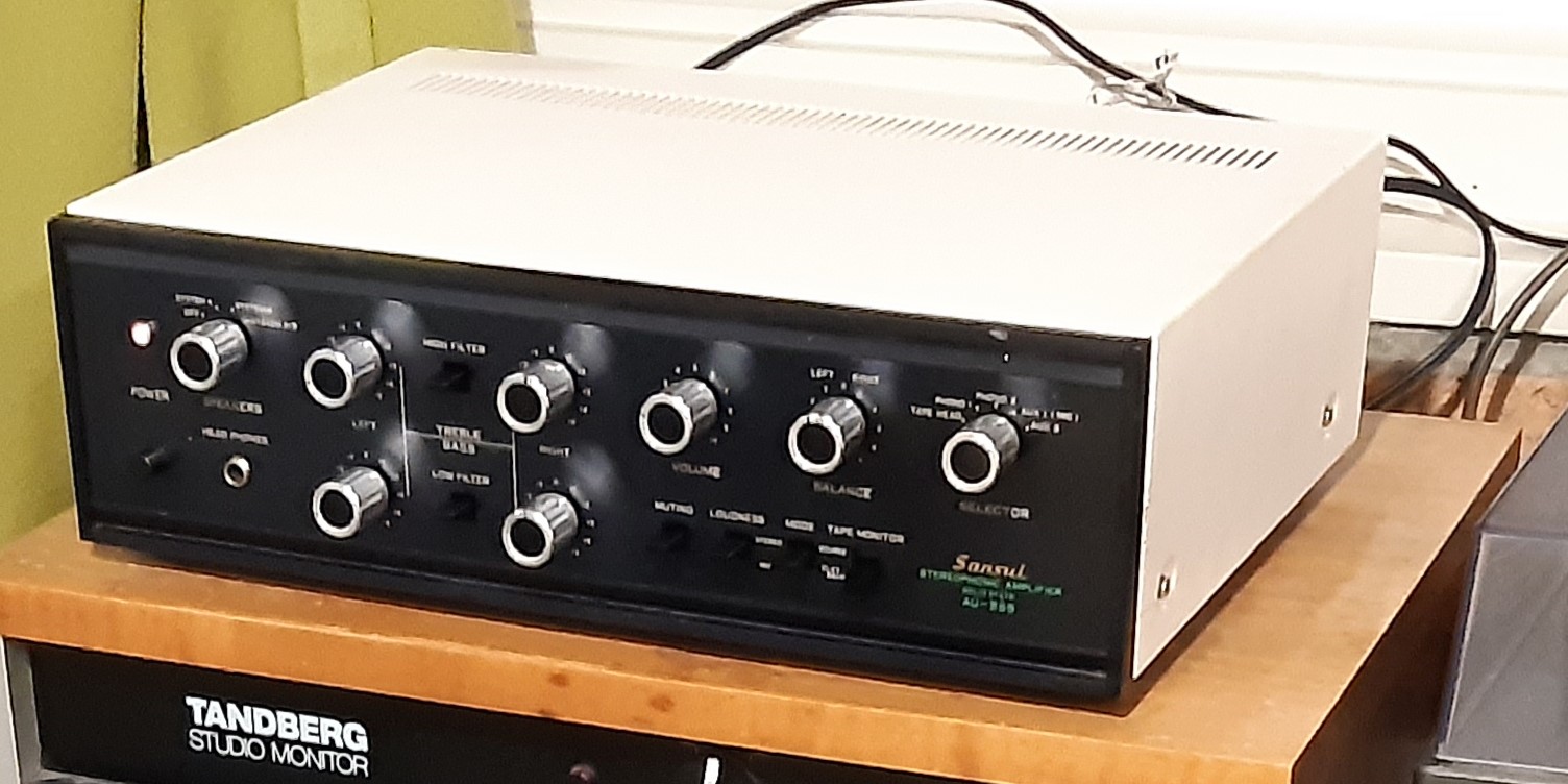
My Sansui AU555, finished January, 2025 .
As usual, I bought this amplifier off the Dutch marketplace, it was sold to me as missing one channel.
Also as usual "somebody was in there before" and this somebody was probably not the first one.
Initial switch on showed this indeed was the case. The preamplifier appeared still working. On the main amplifier card there was a flash at a fuse position at initial power up ;-) . The fuse was sitting loose on one side, triggering a spark.
At the outside, the amplifier appeared to be in a reasonable shape, there is a little "stain" on the metal knobs. A few deteriored spots are on the top of the metal frontplate, and rust on the bolts.
Next comments are aimed at people having technical knowledge, also assuming they gather schematics etc from the net.
![]()
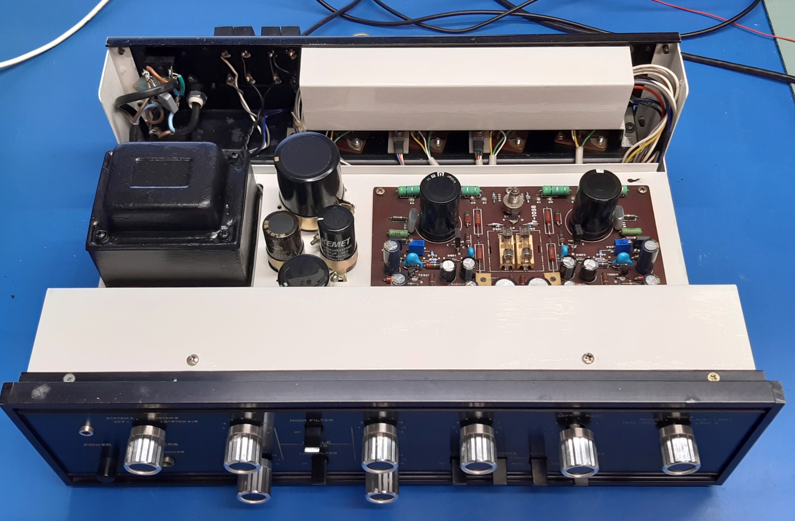
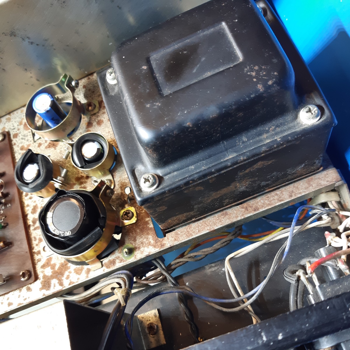
These are pictures of the AU555 innards, before it's refurbishment.
At the back of the unit, rust on the bolts was visible, so it was surprise to see it rusty inside, too.
The amplifier appeared recapped, but apparently without the desired result, probably by some "Sansui Expert". But who am I to judge, in the end because of this I had the chance to buy such as "Recapped, but needs a 'little' attention"
The mains power wiring to the power switch inside looked a little bit unsafe, it would be better to fix up, a bit.
Obviously, a lot of old 10% tolerance resistors were used in the amplifier, in the power sections mostly composite carbon ones, which go up in resistance over the years.
In the end, this amplifier is around 55 years old!
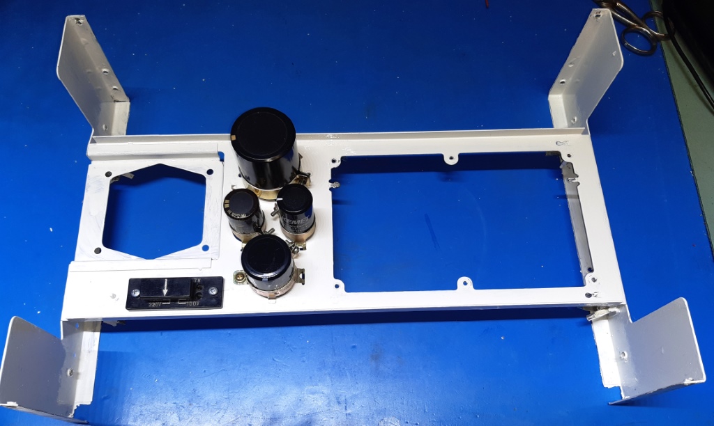
Not being good at metalwork and unable to totally get rid of the rust by sanding the metal, I decided to paint the mid frame. This is how it looked, the frame-mounted power supply capacitors I intended to use are already there.
![]()
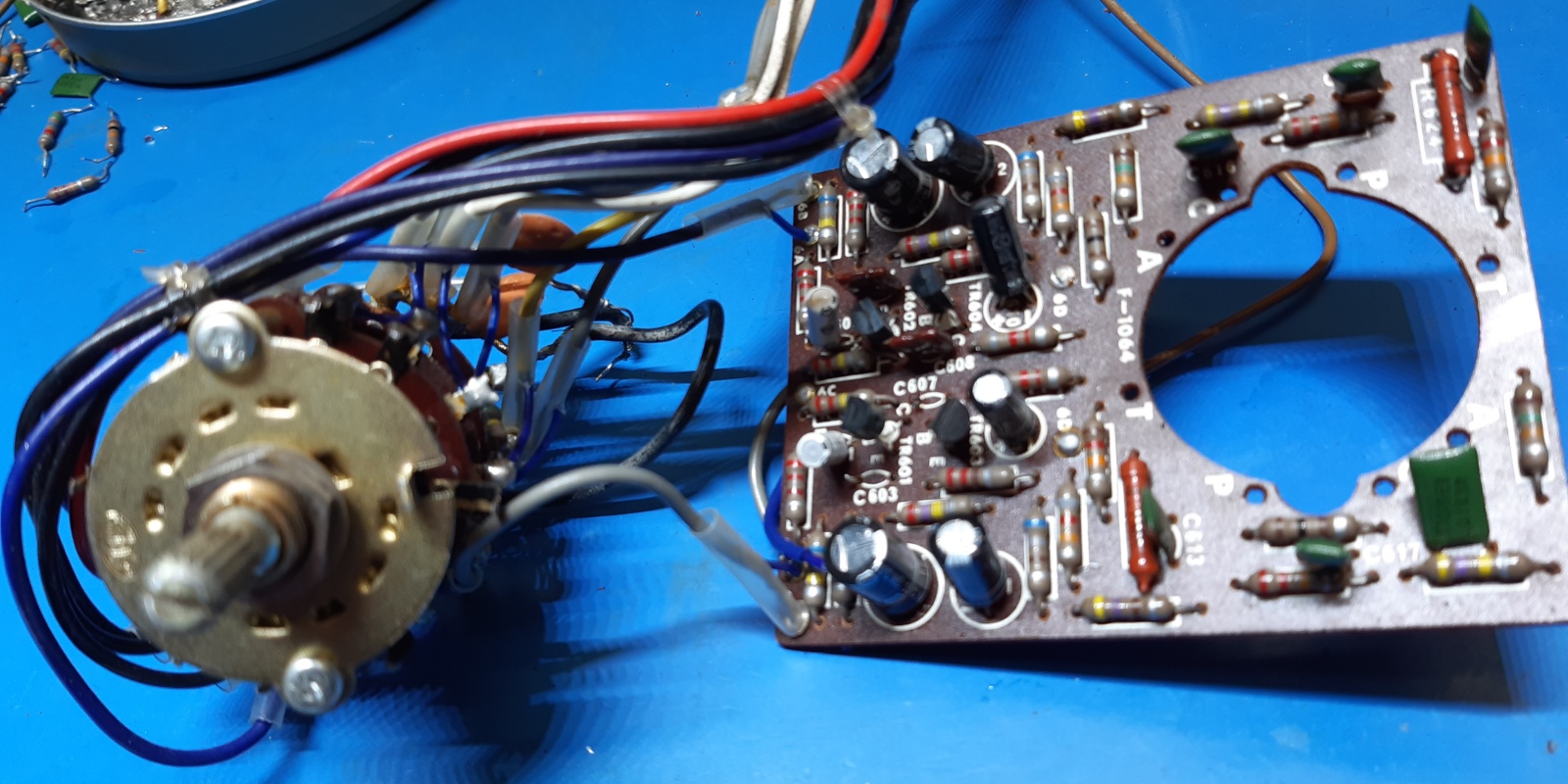
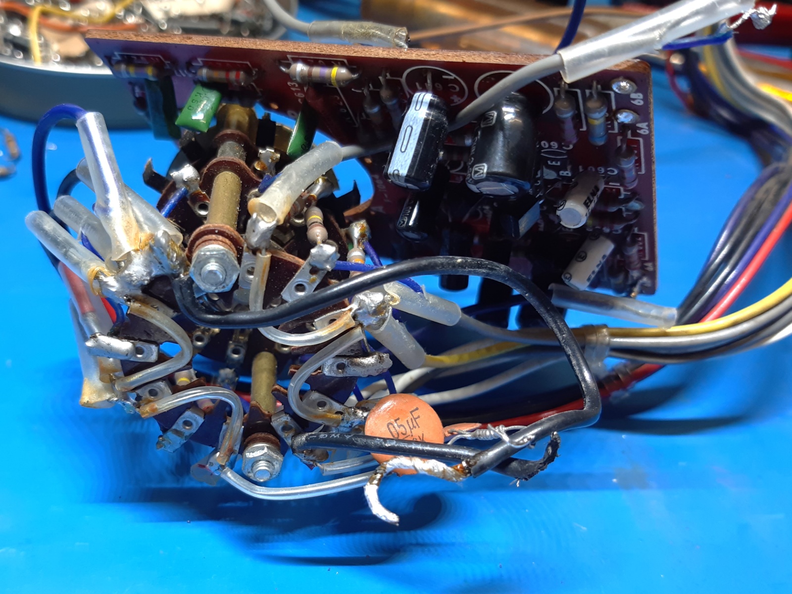
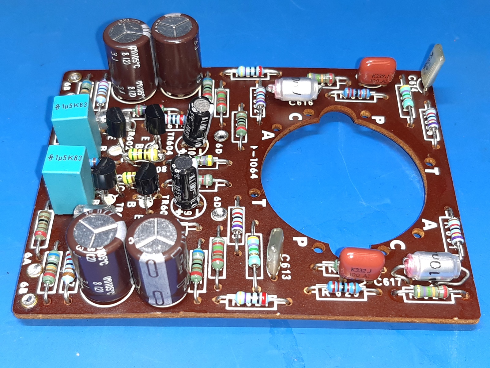
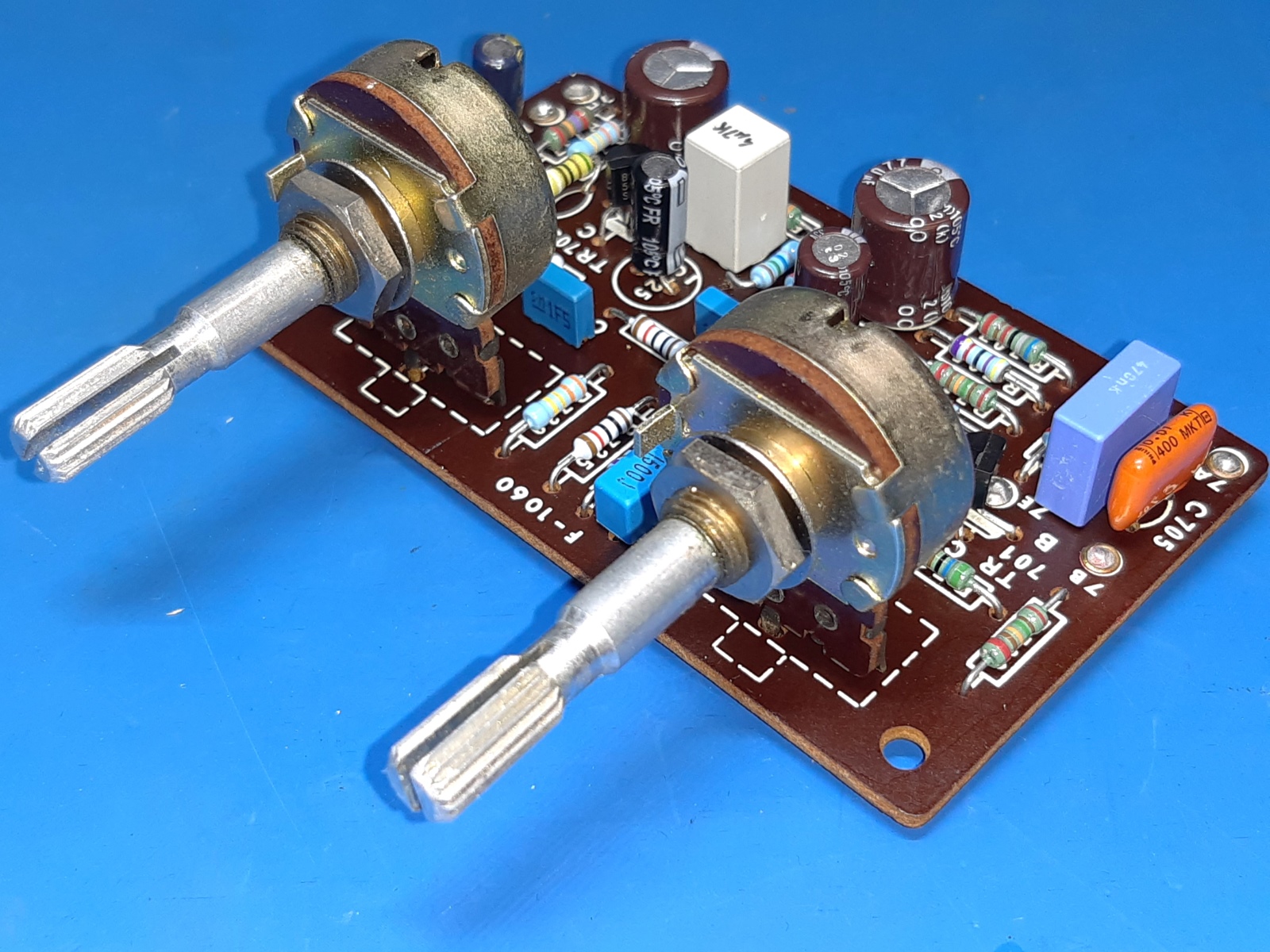
The Head amp F-1064 / pre-amplifier
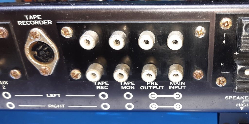
This card is mounted on the source selector rotary switch, it has cabling to frontplate switches and to RCA connectors at the back of the amplifier.
It appears to be a rather messy construction, a challenge by itself.
A rectangulare opening in the frontplate of the chassis leaves a measurement/limited repair possibility.
Probably a long time ago, the transistors were replaced by BC238, maybe the always crappy 2SC458 transistors did give problems in the old past, already.
Also the electrolytic capacitors were replaced by types, which may have existed some 20 years ago, on THIS board only. As the card will be rebuilt, these will not be reused.
Now a "less smart" way of designing is let this preamp also process the AUX 1 and AUX 2 inputs, by first attenuating the signal and then amplifying again, but this is just the way it is.
Sansui corrected this in it's successor, the AU-555A .
There is a way to circumvent this, but it implies reassigning the RCA connectors at the back, wire rearrangements, etc.
As this amp may be sold one day, I leave this as is, for now. The only difference is some resistors changes at the AUX inputs and 20% more feedback leading to less unneeded amplification.
The pictures show how it looked.
I swiped off the components from the circuit card, and I replaced all resistors by the same values which were on the card and the rotary switch already. As a sidenote: the original resistors were 10% tolerance, the new ones have 1% tolerance!
I did put in new BC549 transistors.
The next pictures show the new situation. As stated: All electronic parts are replaced.
After the refurbishment, initially, the amplifier appeared to be "motorboating".
According internet info, alike problems were with other Sansui amplifiers. The solution was lowering the base resistor value providing DC current for the first transistor, values down to 150k were mentioned. Probably the very high HFE of the new BC549 contributed to this motorboating (a slow 0.1 Volts DC movement on the collector of the second transistor.
It appears, Sansui did a modification already, as two versions of these resistor values appear in the documentation. The Service manual shows 470 kilo-Ohms, the schematic shows 270 kilo-Ohms, probably depending on using a newer higher HFE transistor.
This amplifier appeared to have 270k, I did get rid of the problem by mounting 680k resistors parallel from the solder side, the result being some 200k Ohms. The problem was gone.
I do not know, if the 20% reduction of the 15k feedback resistor (to 12k) was also contributing to the problem, initially. Better adapt a resistor to the new high HFE transistor put in, than compromising on noise level.
The resistor reduction leads to the oversensitive amp to be a little "less oversensitive", without compromising its operation.
Anyway, the way it is now, it is probably superior over the original.
![]()
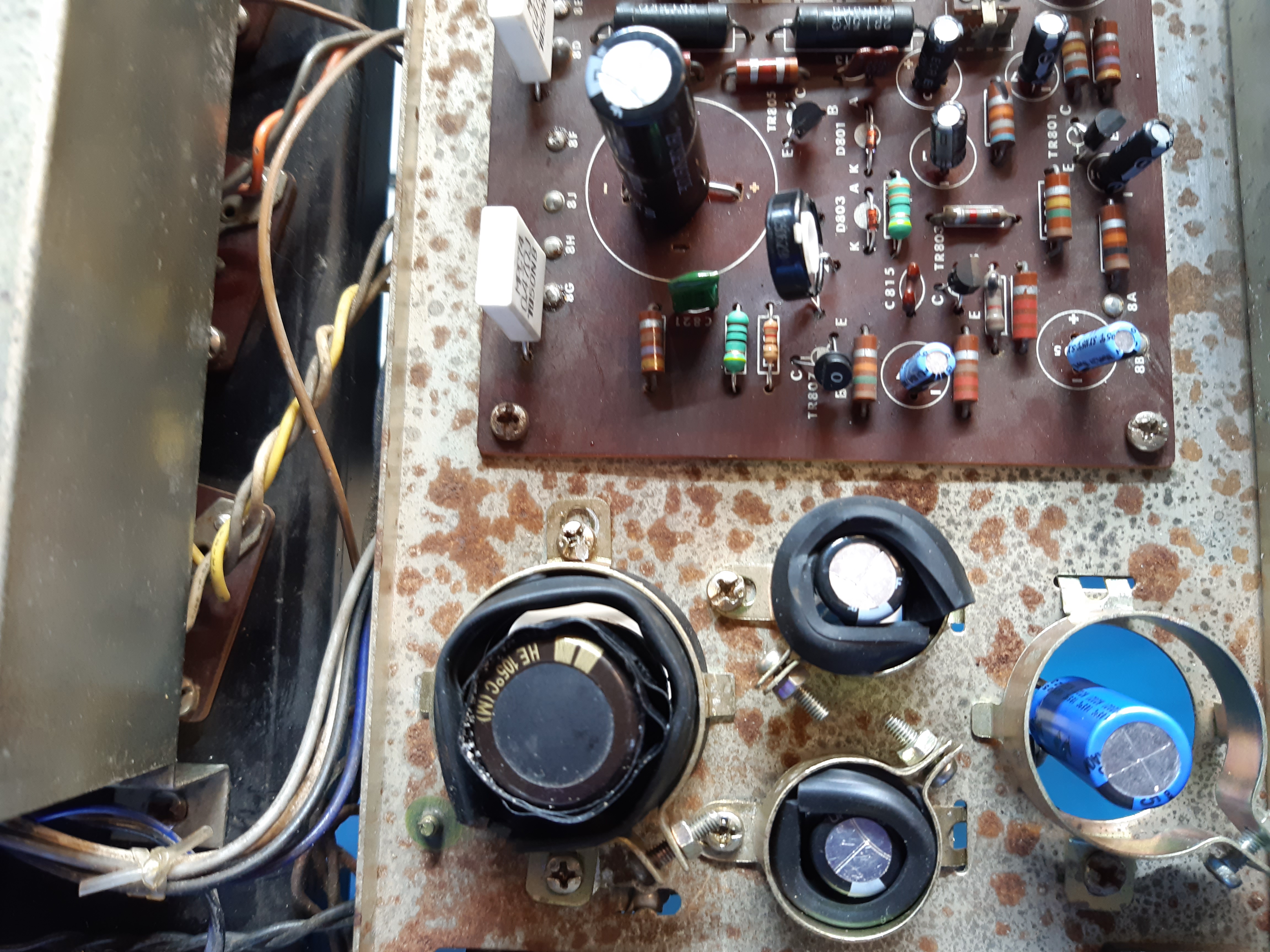
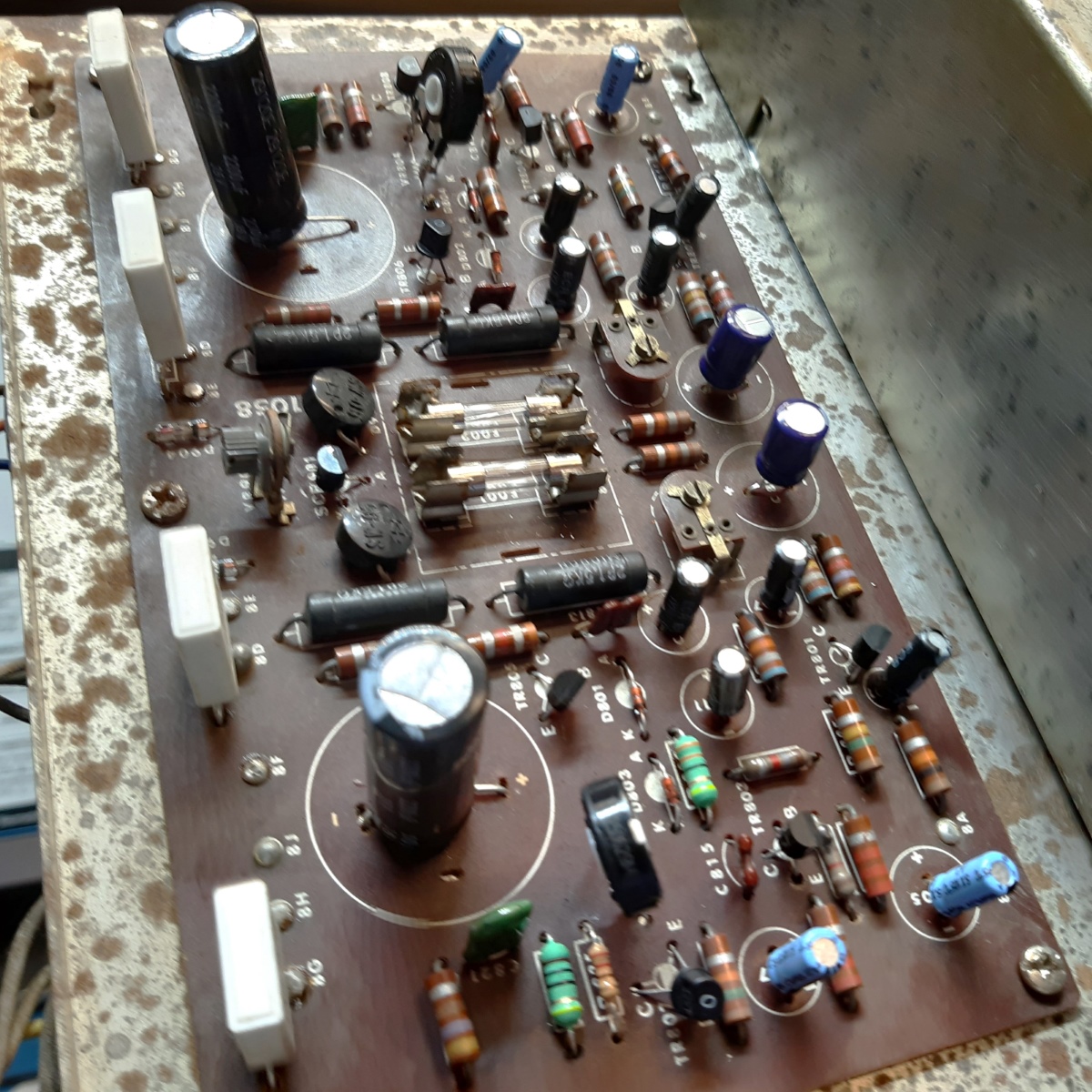
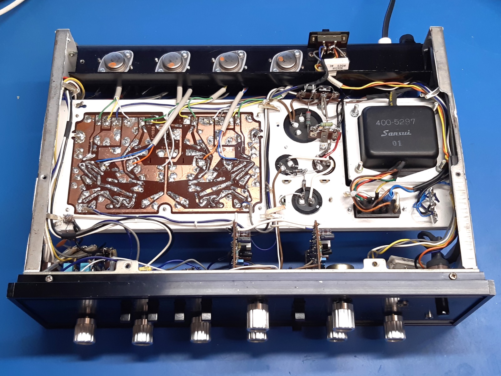
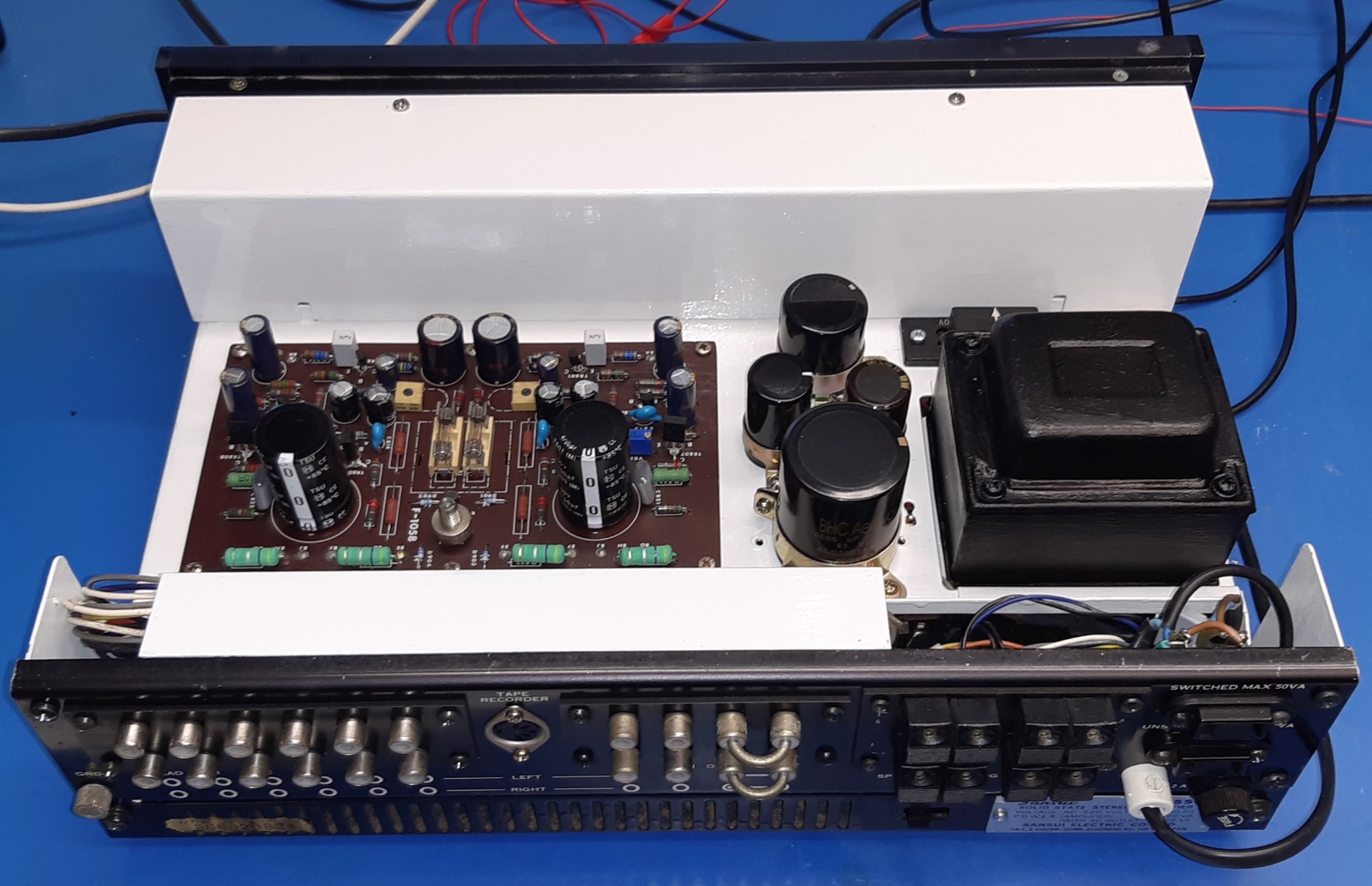
The main amplifier card, F1058.
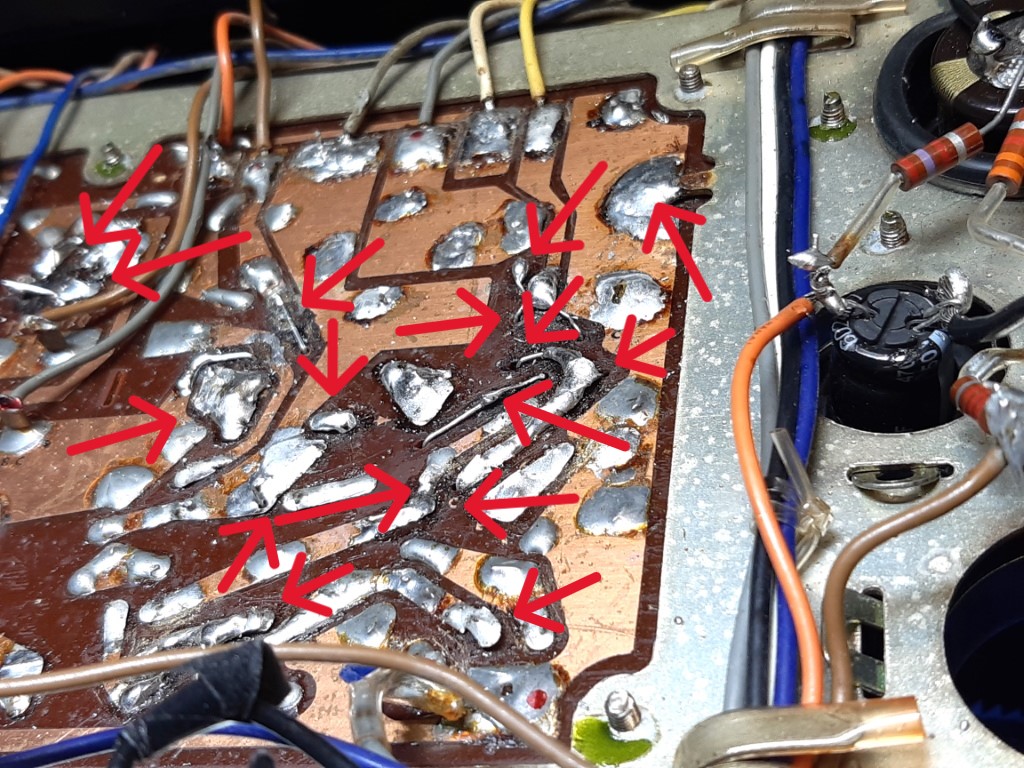
The main amplifiers appeared to look like one big mess on the solder side. Both channels were repaired before, they were recently recapped as well, judging by the part types used.
On the solder side of the card, many pieces of copper tracks were cracked, burnt, or missing.
One more extra total component swipe will not make it look better on the solder side, but technically better only.
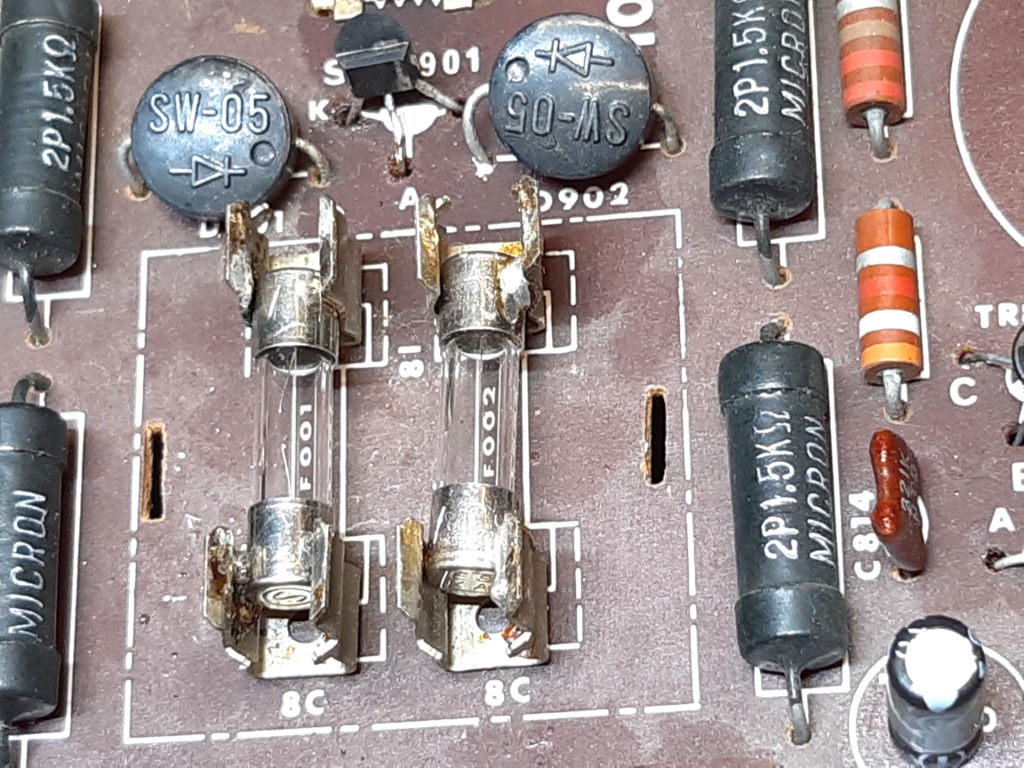
Apparently, the two fuses were soldered in, maybe due to have it transported one soldering cracked and was the reason for the flash at first poweron, the fuse was burnt, afterwards.
Soldering fuses to their holders clearly indicates the type of workmanship (and also, wearout of fuse holders indicate a lot of, or careless use).
There was no other way than rebuild the card totally......
The red arrows reveal most of the circuit track defects found on this part of the card. Trying to remove all the solder, also some remaining pieces of tracks went with the solder.
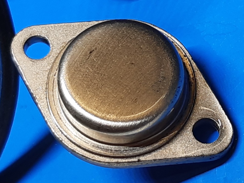
The TO-3 output transistors of the main amplifiers, NEC 2SD180.
One of the NEC 2SD180 transistors appeared loose, it had its mounting bolts missing. One other looked old. Their HFE was very low.
Two shiny transistors did have high enough HFE of around 80, but how become 2SD180 NEC transistors look like new? The lettering on them looked suspicious.
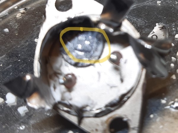
I did put a little IPA on one, and I just could wipe off the text, they are FAKES! They are definately not NEC 2SD180! (ALL new 2SD180 will be fakes as people look for them for decades, already...)
Out of curiosity, I opened one up.

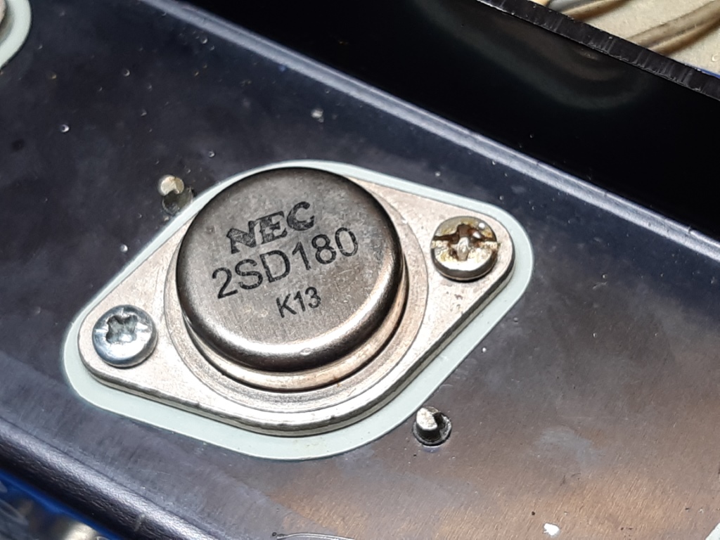
I decided to replace the output transistor by (used) Motorola MJ15024. A bit of overkill does no harm. They are all tested for sufficient HFE.
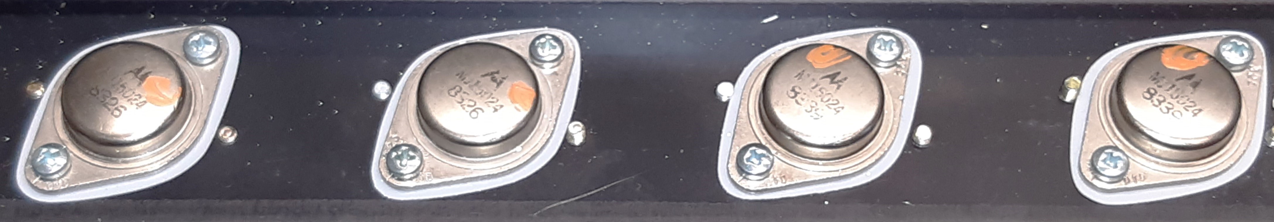
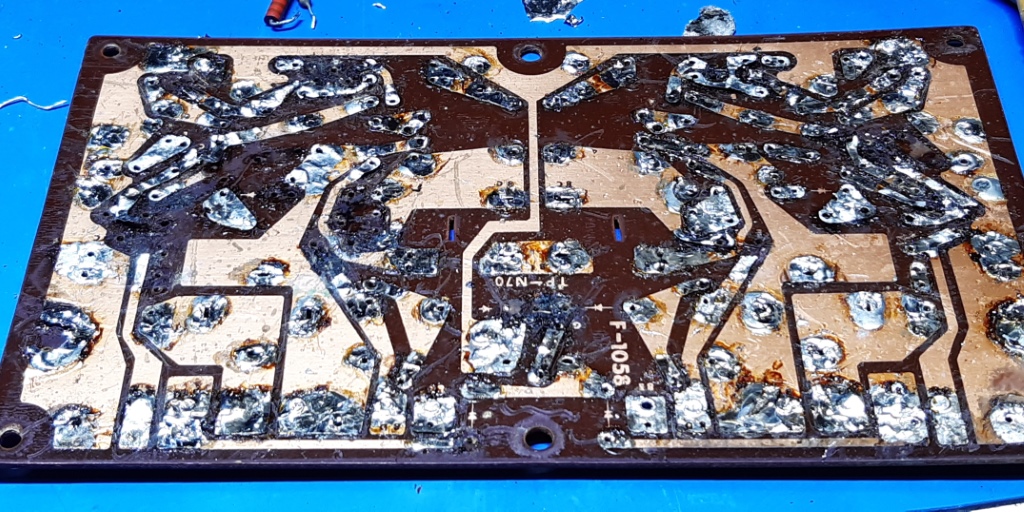
How the card looks after refurbishing.
Parts choice depended on what I had on-hand.
Nice to know is the loudspeaker coupling capacitors are 4700 microfarads, and other electrolytic capacitors also have double capacitance versus the originals.
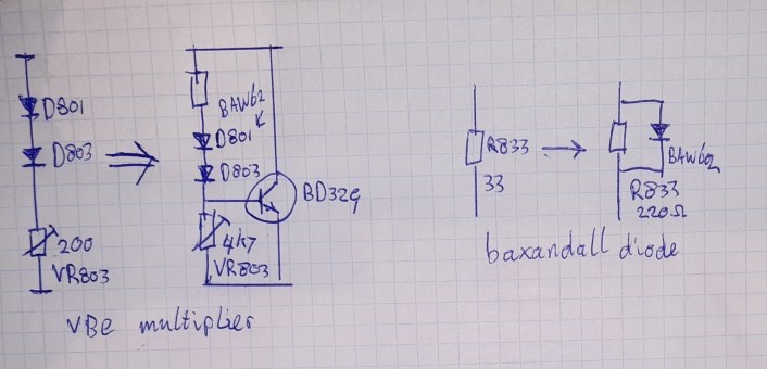
The input transistors are KSC1845, the VAS (voltage amplification stage) transistor KSC1009, VBE multiplier BD329, drivers KSA1220/KSC2690, power output transistors MJ15024 as stated above.

I Incorporated a so-called "baxandall-diode" in the main amplifier circuits. As this modifies the bias settings, the circuit has to be adapted. I did choose to use a TO126 type transistor, because it can be mounted on the heatsink. I decided just to use one of the corners of the TO-3 mounting pads for the power transistors. I used rectangular TO-220 insulating but heat-conducting ceramic washers to mount them on, ensuring good thermal pickup.
The drawing shows the parts of the schematic to be revised. Resistor is 1k8 I think looking at my picture (seeing I forgot to jot down the resistor value on the small drawing).
The modification, including the use of (by me selected for HFE) modern transistors, ensures a distortion (of the main amp circuits) of 0.05% at a very low output, and around 0.02% from 1 watt up to 20 watts, at 1 kHz and 8 Ohms load.
A figure, probably way better than when the amplifier was new.
![]()
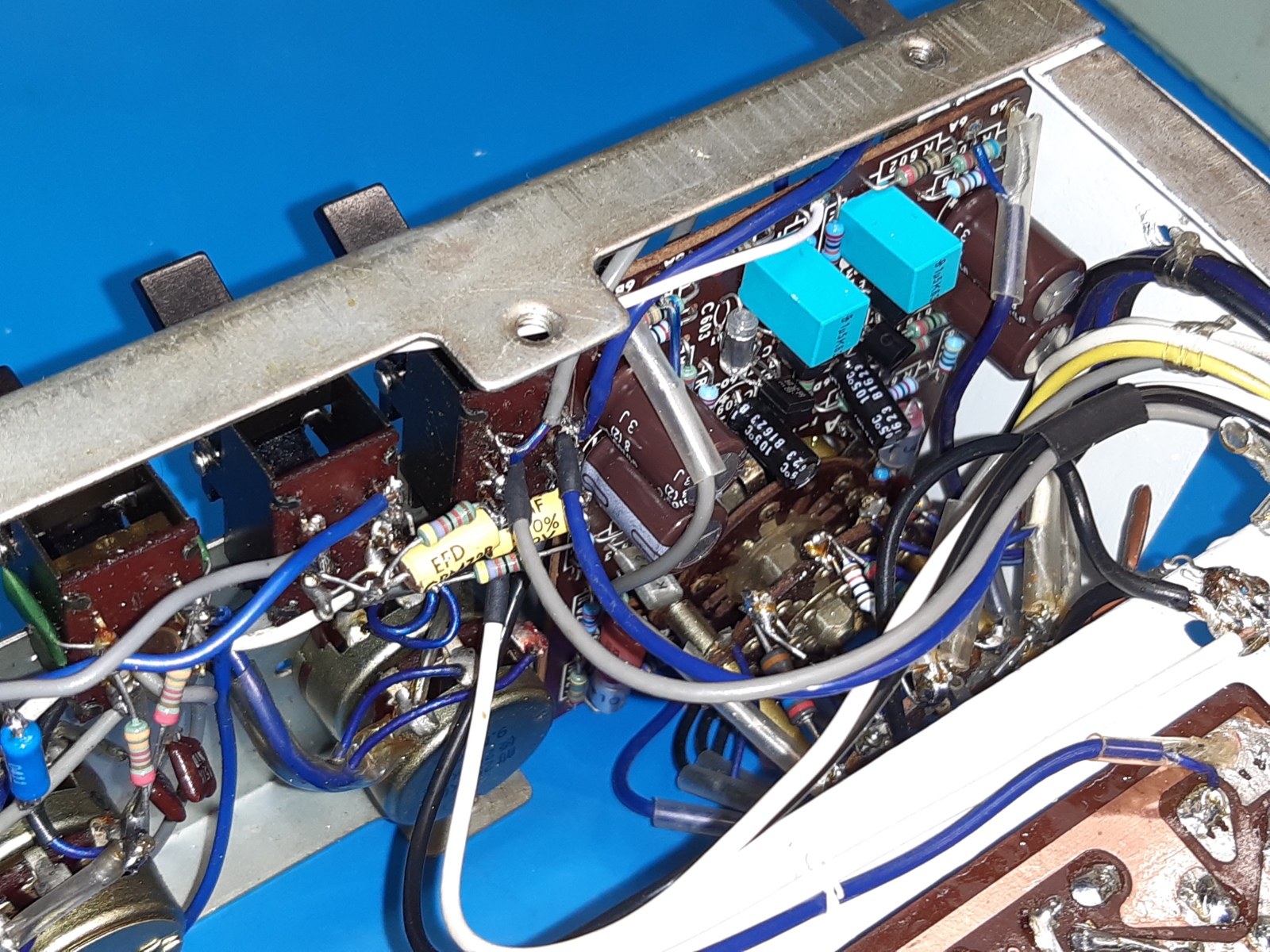
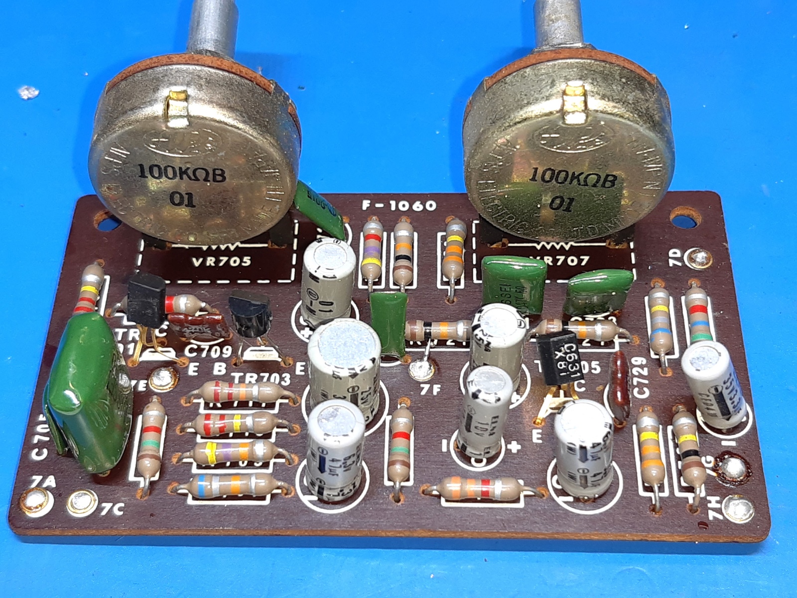
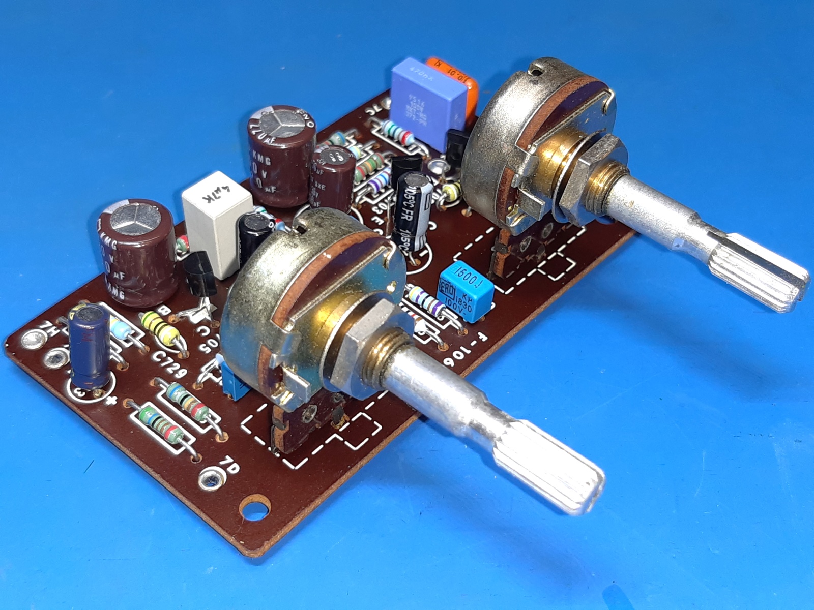
The tone control boards, "control AMP", F-1060.
There are 2 of these, exactly the same. They wer populated still having their original parts. As can be deducted from the picture, all the resistors on it are 10% tolerance ones, to be replaced by 1% tolerance ones.
Being not touched although it looks they once did get a shot of contact cleaner spray, they are in very good shape. Therefore, I did not have any problems refurbishing them.

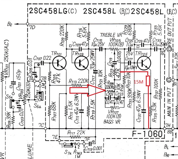
The schematic shows I did put a resistor of 15 megaohms to ground, to provide a negative DC voltage versus both coupling capacitors coming from the input and output transistors going to and from the baxandall tone section. Otherwise, this section is "floating", its DC level depends on which capacitor leaks the most, deteriorating the least leaking one.
I also put an arrow towards R739.
As after refurbishment of the amplifier I felt it was a bit "bass-heavy", which is liked by a lot of people, called the "Sansui-sound".
To me, it just was distracting having to move the bass potentiometer a bit counterclockwise .
Now, this very 330 kilo-ohms resistor creates an abnormal offset in the tone control, enough to be audible. The best solution would be just taking away the resistor, although I will just leave it in and have the bass controls a bit backwards, preserving the "Sansui sound.
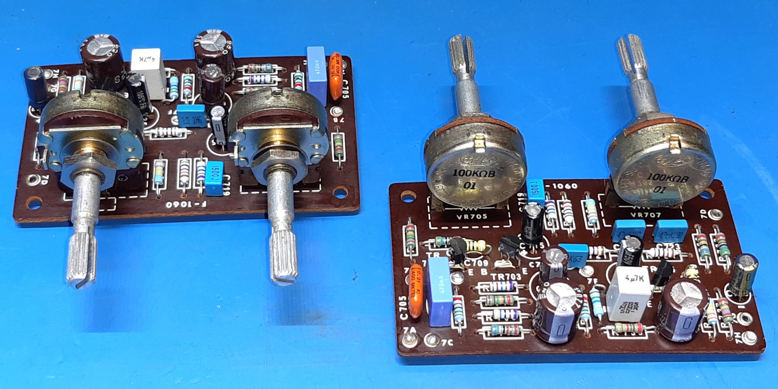
The new transistors are all BC549. Apart from the potentiometers, all parts are replaced.
![]()
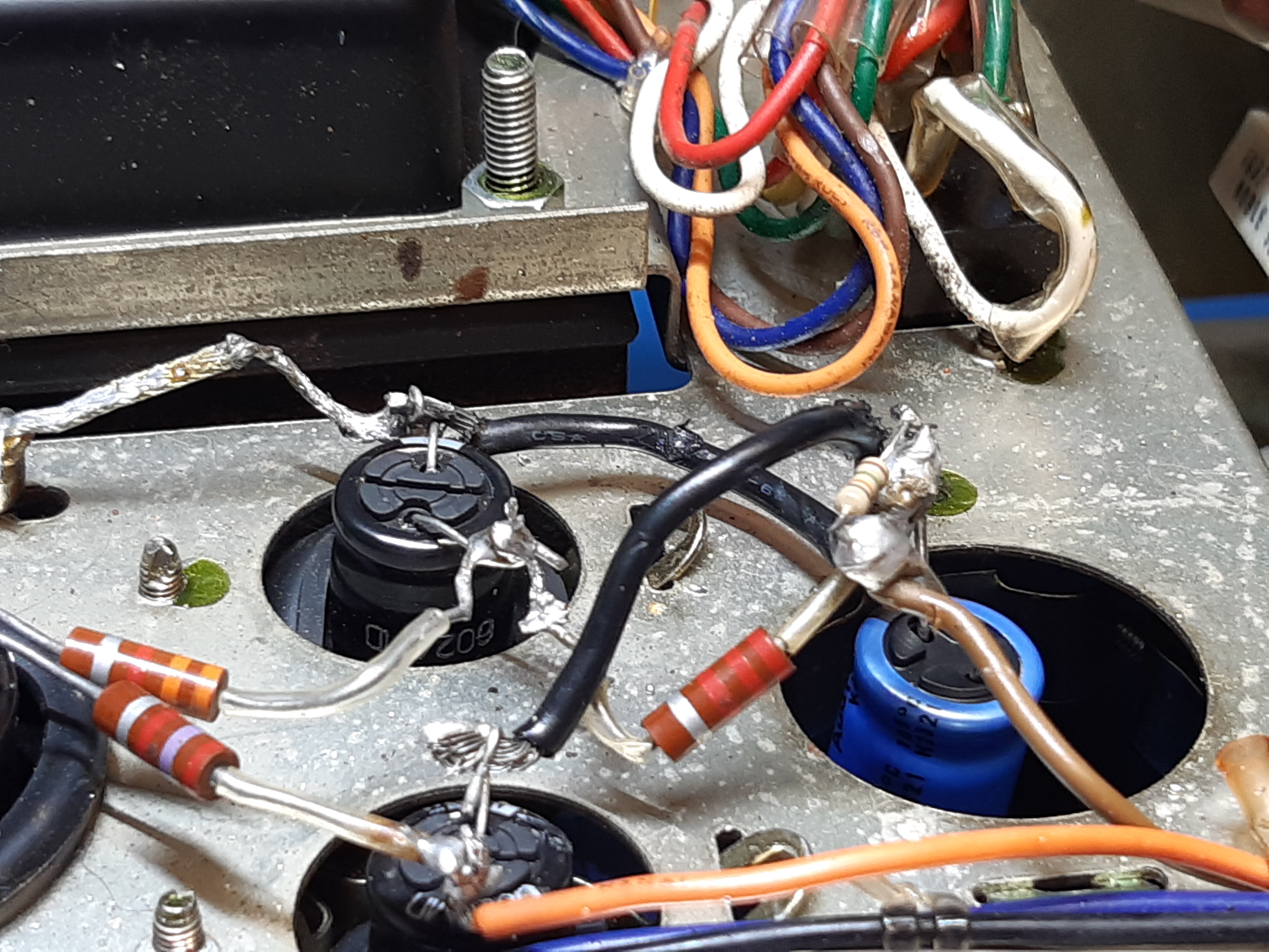
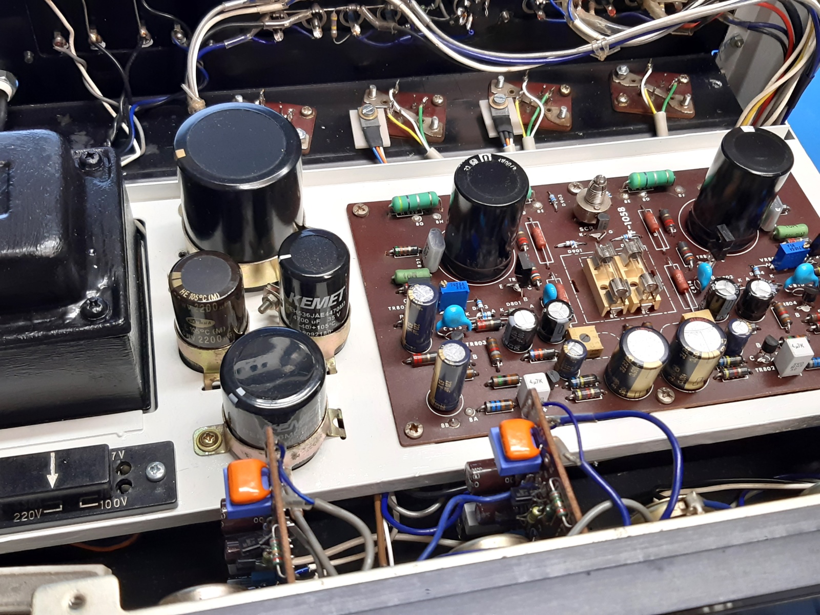
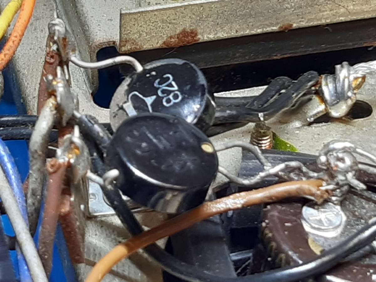
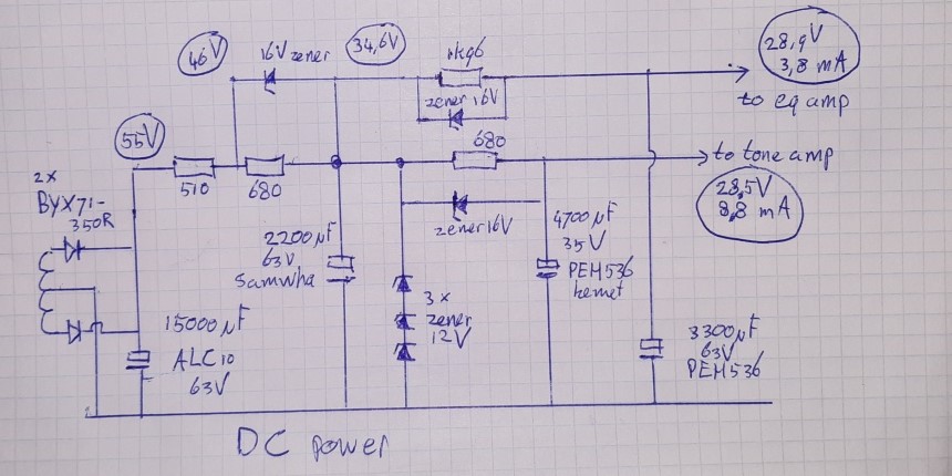
The power supply.
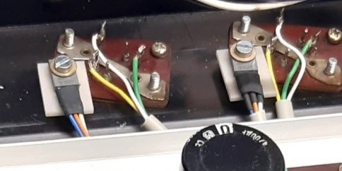
Because of deciding the old wiring was not safe enough, I decided to replace the internal mains wiring. The power switch was rewired, the capacitor on it was moved over to the back of the chassis.
Additionally, on the switched part of the power (read:transformer primary connections) I added a 320 Volts MOV surge suppressor.
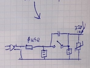
These are pictures of the old and new wiring on the switch.
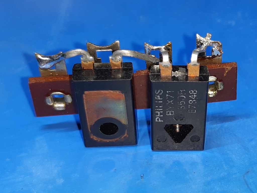
As the biggest power smoothing capacitor will require more peak current from the rectifier diodes, I decided to replace those by Philips BYX71 diodes, which I have on hand. The original situation had disc type diodes looking quite different, although the BYX71 ones look odd, also ;-)
The picture shows, a 4-way mounting strip was used instead of the old 3-way one. On the left, the old situation, on the right, the new diodes, before soldering.
The power DC supply did get some changes. One goal was use the correct physical size capacitors, another was better power smoothing. Capacitors I had on hand were used.
As the capacitances are much higher now, I made an arrangement with Zener diodes to keep the initial charging up fast enough, as one does not want to wait a minute or so until until charge is enough to have sound....
I presume the small power transformer will limit current enough to make the change not hazardous for the power switch.
C002 the big one, ALC10 15000 uF /63V , instead of the original 2000 uF.
C003 2200 uF 63V,Samwha it used to be 500 uF.
C004 4700 uF 35V PEH536, it used to be 1000 uF.
C005 3300 uF 63V PEH536, it used to be 500 uF.
Not putting pictures of them here, as they are visible as part of several other pictures.
The schematic below shows the new smoothing capacitors, resistors, and zener diodes situation, it is very much different from what it was. It should be noted, all 16 Volts zener diodes are only present to speedup charge, once the capacitors have a reasonable charge voltage, the voltage over the zeners is lower than zener voltage so they are "turned off".
Apart from that both preamp sections are fed from a capacitor coming from the intemediate smoothing capacitor C003, which has three 12 Volts zeners in series to get an around 36 Volts charge. The 510 Ohms resistor together with the 16 Volts zener diodes set the limit of initial current to C003,C004 and C005.
This current is a bit variable, as the measured input voltage on C002 varies from 53 to 55 Volts, depending on the mains voltage "out of the wall"
![]()
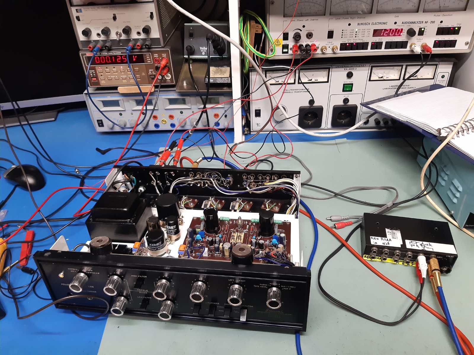
Testing the main amplifier section.
The main amplifiers on the amp board were tested on a Burosch NF200 analog distortion analyzer, capable of testing 0.1% full-scale, 1 kHz only. This device has an internal sine wave generator and 8 Ohms shunts to mimic a resistive load.
The results were, both channels same ouput and distortion about the same at both:
-50 Milliwatts : 0.04%
-1 Watt: 0.025%
-10 Watts: 0.02%
-20 Watts: 0.02%
This is a VERY satisfying outcome!
Originally, without the "Baxandall diode modification", it probably would be higher, as this modification is supposed to lower power amp distortion with some 50%.
The distortion meter has two meters on the left indicating some 20 Watts on the picture (the 200W second scale) and the mostright is distortion on the left channel at that moment as indicated by the green led, on the selected 0.1% fulle scale indicating 0.03% (signal generator itself adds around 0.01% also)
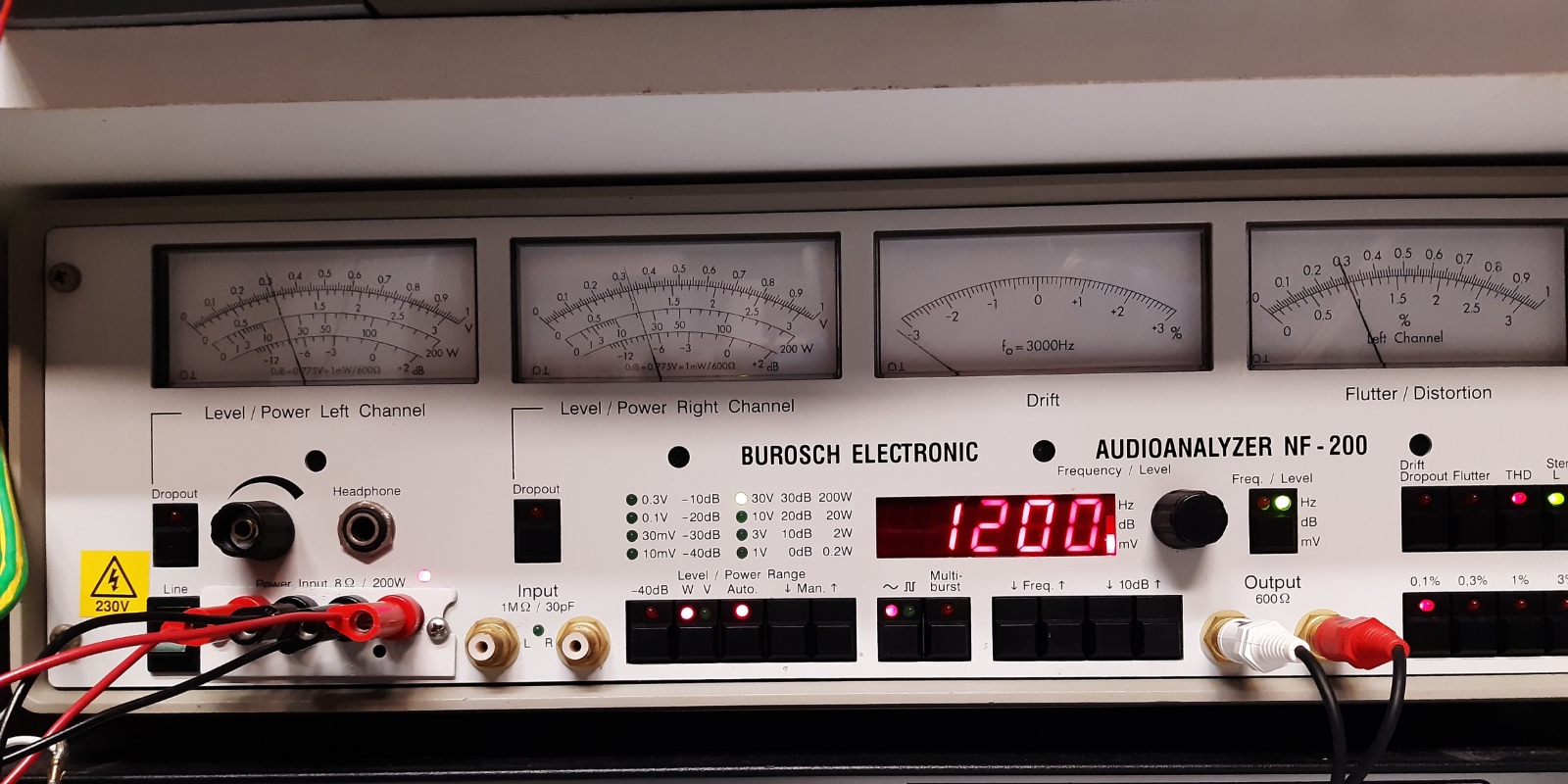
The measured maximum power before clipping and a rising distortion was 21.5 Watts per channel (1kHz)
Some more observations to ADJUST the amplifier, regardless of what the service manual states:
Adjust the bias current:
The Current Bias voltage over the 0.47 Ohms emitter resistors, when the heatsink was around 33 degrees C left and around 38 degrees Celcius on the right: 13 mV both sides, after taking some time to do the measurements done.
NOTE: the temperature difference exist because of on the left side there is much better cooling, there is simply more metal available for cooling!
The bias voltages were about the same as when the amplifier was cold, so the installed "VBE multiplier" circuit proved it works well.
Adjust the balance trimming potentiometers:
Raise the input 1kHz voltage until the amplifier is just visible on an oscilloscope (a normal one not tiny elcheapo playtool)
Set the balance trimming potentiometers to a position the clipping is same at the positive and negative side of the sine wave.
On this amplifier, in this situation the DC power sagged until 47.4 Volts. DC Voltage measured at Collector of lower pair after adjusting the balancing trimmers: around 23.15 Volts.
Of course, this measurement is to be taken having the amplifier loaded with 8 Ohms. If one has 4 Ohms loudspeakers, one will have more power sag, so the adjustment will be different to enhance maximum power at 4 Ohms.
The 47.4 Volts is due to power sag at high output. Putting the input signal back to zero, the DC Voltages were 55 and 24. It is quite clear how much the maximum power affects the DC voltage.
![]()
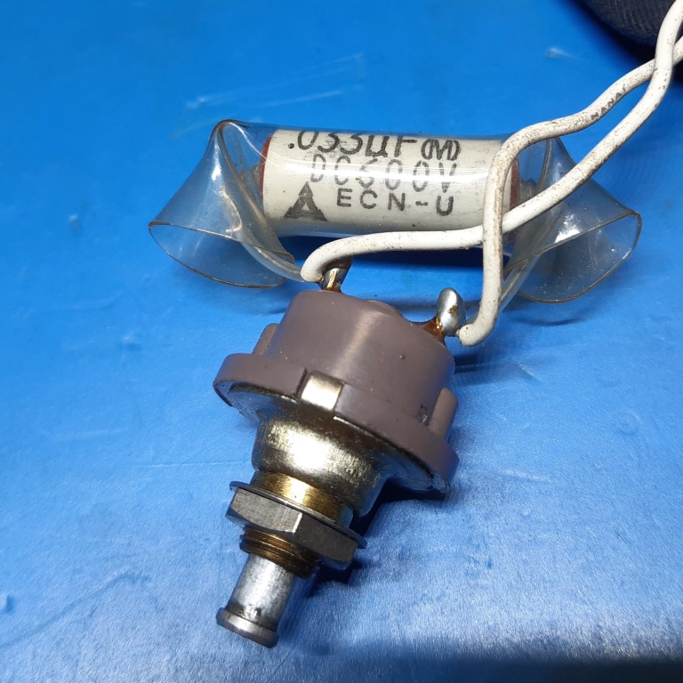
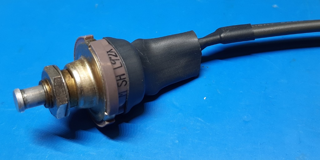
Various pictures.
On the back of the unit and elsewhere, just about all bolts were replaced by ones not carrying rust. Also, the 5-pin DIN tape connector socket was replaced.

![]()
Ga naar Gerards page / go to Gerards other pages ---->>> ![]()